


Mobile phones today have been transformed from mere communication devices to pocket-sized computing machines in the digital age. But hiding beneath the sleek exterior and high-definition screens is a complex array of pieces that enable this feat to occur — the Printed Circuit Board, or PCB.
What is a PCB?
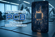
Cellular phones and almost all other electronic devices depend on a Printed Circuit Board or PCB, for their structure. The non-conductive material used for the board covers, holds and connects the different electronic components using copper-etched tracks and pads. PCB technology uses different layers which are based on how sophisticated the equipment is. Multi-layer PCBs are often found in cell phones since they are both small and can be designed for complex functions.

Role of PCB in Mobile Phones:
1. Centralized Component Mounting
The PCB is a central platform on which all the electronic components, including processors, memory chips, SIM card reader, antennas, and sensors, are mounted. It gives the components the necessary physical support and electrical connections through soldered joints and copper tracks.
2. Compact and Efficient Design
Smartphones require ultra-miniature and high-density component arrangements. Multi-layer PCBs enable mobile makers to integrate several layers of circuits in a small package with both miniaturization and efficiency.
3. Signal Routing and Power Distribution
PCBs ensure correct signal routing among processors, RAM, storage, cameras, and external interfaces. They also provide regulated power to each module to sustain stable performance without the loss of energy.
4. Thermal Management
Mobile phones produce heat when in use. Contemporary PCBs employ materials and design methods (such as thermal vias and copper planes) that allow effective heat dissipation to avoid damaging delicate components.
5. Mechanical Strength and Durability
PCBs offer structural integrity to the phone. Designers can couple flexibility with durability through rigid-flex PCB technology, supporting foldable screens and curved designs while ensuring electronic reliability.
Advancements in Mobile PCB Technology
The continually accelerating advancements in smartphones — with 5G, great-shoot multi-lens cameras, facial recognition, biometric authentication, and AI-based features — have led to an urgent need for smaller, more efficient, and highly powered circuit boards. By the same token, mobile PCB technology has also come a long way. Let's discuss the most significant developments that are shaping mobile device design in the years to come:
1. HDI (High-Density Interconnect) PCBs
HDI PCBs have smaller vias, thinner traces, and tighter spacing, enabling designers to integrate more functionality into smaller spaces.
Why it matters: Contemporary smartphones have sophisticated processors, memory modules, and RF components — all of which must be heavily integrated.
Benefits:
- Quicker signal transmission
- Less signal loss and electromagnetic interference
- More layers in a smaller size
Use cases: Main logic boards of high-end smartphones, 5G modem integration, AI chipsets.
2. Flexible PCBs
Flexible PCBs (FPCBs) are built with flexible materials like polyimide, which fold and bend without failing.
Why it matters: As foldable smartphones, wearables, and small form factors become more popular, rigid boards are no longer sufficient.
Benefits:
- Light in weight and space-saving
- Ideal for curved or mobile components (e.g., hinge regions of foldable phones)
- Greater longevity over time with less mechanical joints
Applications: Foldable screens, camera modules, antennas, wearables fitness trackers.
3. Substrate-Like PCBs (SLP)
SLP technology applies sophisticated semiconductor-like processes to produce ultra-thin PCBs with very fine lines and spaces — usually below 30 microns.
Why it matters: SLPs enable next-generation chips and thinning of mobile devices without compromising power or functionality.
Benefits:
- Thinner and lighter smartphone bodies
- Enhanced electrical performance and design freedom
- Facilitates miniaturization of critical internal systems
Applications: High-end smartphones such as Apple iPhones and Samsung Galaxy S-series.
4. Embedded Components
In this process, components are not mounted on top of the PCB but are embedded within the board layers.
Why it matters: With mobile phones needing greater power and functionality within lesser space, embedding components conserves surface area and increases speed.
Benefits:
- Optimization of space
- Shorter signal paths for greater speed and efficiency
- Better thermal and electrical performance
Applications: Power management ICs, capacitors, RF components in mobile system boards.
Why PCB Quality is Critical in Mobile Manufacturing
In cellphones making, Printed Circuit Board (PCB) quality is not only a technical issue — it is a key to product dependability, consumer satisfaction, and corporate prestige. Since PCBs act as the heart in powering, regulating, and interconnecting all the internal elements of a mobile phone, even the smallest defect can lead to serious problems.
Let's discuss the implications of low-quality PCBs and why there is a need for precision and quality control at each step.
1. Device Failure or Overheating
Misaligned vias, poor insulation, or defective copper traces result in current hotspots or unnormal current flow, respectively, and cause overproduction of heat. With prolonged usage of the device, sensitive parts like the battery or processor get damaged and lead to shutdown or, in extreme conditions, fire.
2. Decreased Battery Life
High-resistance paths, leakage currents, or poor power distribution due to PCB defects may consume the battery faster. Customers would likely experience their phones no longer lasting throughout the day, which negatively affects the mobile experience and may lead to higher return rates and warranty claims.
3. Erratic Performance
Low-quality PCBs can cause signal integrity distortions, generating random system crashes, app malfunctions, touchscreen malfunction, or sluggish performance. In mobile devices that operate on high-speed processors and real-time wireless connectivity, any form of instability in the PCB directly worsens overall usability.
4. Total Device Failure
In extreme circumstances, a faulty PCB can lead to a phone that does not work at all from the box. When power rails are shorted, important components are detached, or solder joints collapse when the equipment is used, the gadget might go entirely dead, necessitating replacement or repair.
Why Quality Assurance Is Important
Considering the possible risks and effect on user experience, major mobile makers have in place stringent quality control procedures, such as:
- Automated Optical Inspection (AOI) to catch soldering defects and misalignments
- Electrical Testing to check for signal continuity and levels of resistance
- X-ray Inspection for internal layers and concealed joints (e.g., BGA components)
- Environmental Stress Testing for thermal, vibration, and drop resistance
- Certification and Traceability by trustworthy PCB suppliers
These steps guarantee every PCB can withstand the demands of actual use — from high performance to extended battery life, thin profile, and heat management.
The Future of PCBs in Mobile Devices
As smartphones get more intelligent and more powerful, PCBs will keep changing. Future trends are:
- 3D-printed PCBs for quick prototyping and tailor-made designs
- Nanomaterial-based PCBs for extremely thin devices
- Biodegradable substrate-based eco-friendly PCBs
- AI-driven PCB testing for enhanced quality control
Mobile PCB development is going to dominate the future of smartphones, tablets, wearables, and IoT devices.


